[WIP] RFID Explained
RFID is complex but It’s also fun. Personally I find this technology to be a bit underutilized. I’d like to explain it in a simple way so you don’t have to do the “wait, what?” through the many, many documentation PDFs. I hope to give you some confidence and maybe inspire you to do something fun with RFID.
My experience is that you either grab the cheapest, most popular MFRC522 based RFID reader and hook it up to Arduino or you go deep down the rabbit hole. I’d like to bridge that gap. Enough knowledge that you know where to look for the answers and if you put in a bit of work you’ll hopefully be able to write your own driver for a RFID reader. I won’t tell you how to design your own PCB with a custom antenna, which, I agree, is a bummer.
Tags <
The RFID Tag or Card or any shape it chooses is universally called a PICC - Proximity Integrated Circuit Card. Yes, there is a card in the name but no one cares. It’s XXI century. Words mean nothing nowadays. The, very popular, blue keychain tag is also a PICC.
A PICC is generally defined by the ISO/IEC 14443. There are two types described by this standard Type A and Type B. The main differences between these types concern modulation methods, coding schemes and protocol initialization procedures. The standard is described in four documents:
- ISO/IEC 14443-1:2018 Part 1: Physical characteristics
- ISO/IEC 14443-2:2016 Part 2: Radio frequency power and signal interface
- ISO/IEC 14443-3:2018 Part 3: Initialization and anticollision
- ISO/IEC 14443-4:2018 Part 4: Transmission protocol
If you want to read those standards you have to buy them. Why do we sell standards? It’s ridiculous.
The Type A is the most common type. Usually you’ll see it referred to as ISO 14443A.
PICCs in the wild <
Standards, as exciting as they are, are just documents which describe a list of requirements one should adhere to, to be able to say that their product is actually that thing that the standard describes. “Dog is a fluffy, wholesome creature, which is always there for you” - according to this standard a cat can’t be a dog even though it meets some of the criteria. Let’s look at some PICCs that do their best to satisfy ISO 14443A requirements.
MIFARE <
If you want your products to work with the RFID technology you should stick to the ISO 14443 standard. There are some parts of it you can ignore and things will still work. Maybe your dog doesn’t have to be fluffy. NXP Semiconductors introduced their own implementation of the ISO 14443A standard, called MIFARE.
There are different families of MIFARE PICCs and those comply with different parts of the ISO 14443A. The most common family is the MIFARE Classic:
Employs a proprietary protocol compliant to parts 1–3 of ISO/IEC 14443 Type A, with an NXP proprietary security protocol for authentication and ciphering. Subtype: MIFARE Classic EV1 (other subtypes are no longer in use).
More importantly:
The MIFARE Classic IC is just a memory storage device, where the memory is divided into segments and blocks with simple security mechanisms for access control. They are ASIC-based and have limited computational power. Due to their reliability and low cost, those cards are widely used for electronic wallet, access control, corporate ID cards, transportation or stadium ticketing.
I recommend scrolling down on the MIFARE Classic website to the Application Board. There are some inspiring examples there.
The rest of the MIFARE’s description is mostly based on the MIFARE Classic EV1 1K datasheet.
Lets move to what the actual MIFARE chip is. It’s a simple state machine, powered with the energy transmitted via electromagnetic waves. That’s what all PICCs are. If you want to control a PICC you change its state using appropriate commands.
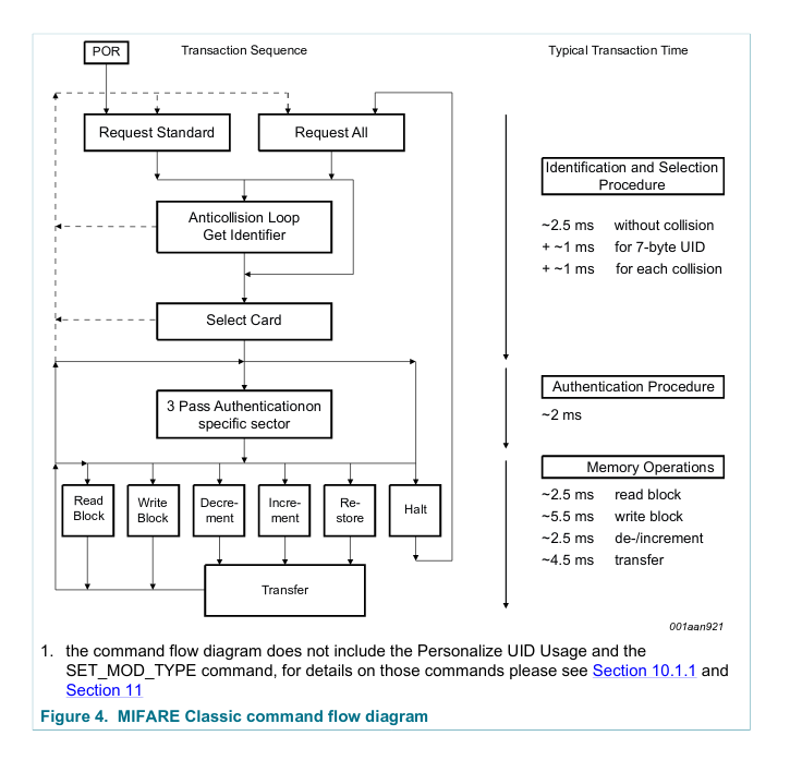
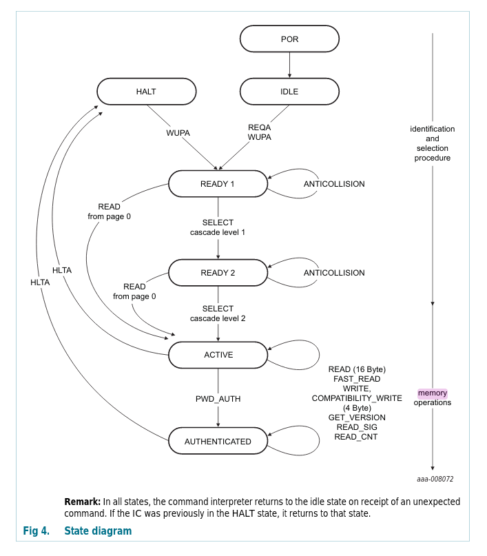
The diagram above comes from the datasheet (p.6) and it’s less than perfect. It tries to show the internal state machine but it focuses on the transitions between those states. It doesn’t even use the common terminology… confusing! Let me walk you through it.
The PICC goes into a POR - Power-On Reset state when it gets enough power. As soon as the PICC boots it goes into an IDLE state (Request Standard). In this state it waits for either REQA or WUPA command to change its state. Another inactive state is the HALT (Request All) state. In this state the PICC will only respond to WUPA command. Why two inactive states?
In a situation in which you want to test for a PICC presence you can transmit the REQA command. If there is a response (so called ATQA response) the PICC moves from IDLE to a ready state. At this point you have to perform few more steps to finally read or write the PICC’s memory. After that you move the PICC into HALT mode (you have to move the PICC into either HALT or IDLE after a read or write operation). Now, you go back to transmitting REQA command. The PICC won’t respond. REQA doesn’t activate a halted PICC. Only WUPA can do that. That is until you move the PICC outside the RF field, basically removing its source of power, and move it back close. That resets it into IDLE state. REQA allows for ‘one operation per one proximity detection’ operation. If you were to transmit WUPA to test for a PICC presence, the PICC would wake up from HALT and you could perform another operation. That way you can continuously communicate with the PICC without moving it back and forth (you might want to do that when formatting the PICC’s memory). You can get the same result by moving the PICC into IDLE state after an operation and transmitting the REQA command.
You can find more in the MIFARE Type Identification document. It’s full of useful graphs and, what’s most important at this step, explanation of the ATQA response. The previous step activated the PICC and everything we know about it is encoded in the 2 bytes of ATQA. Page 8 of the MIFARE Type Identification explains its contents. For example, bit 7 and 8 can tell you the size of the UID (Unique Identifier) of the PICC. The size of the UID can be 4, 7 or 10 bytes. You read that UID during a process called Anticollision.
Anticollision <
This is a process which solves the problem of multiple PICCs in the RF field. The idea isn’t that complex. You transmit an Anticollision L1 (level 1) command. It’s a simple, two byte, message. The PICC responds with its entire UID, if its UID is 4 bytes, or the first 4 bytes if its UID is longer. Part of the response is the CT (Cascade Tag) byte which tells the reader if the entire UID has been communicated. One way or another you have to respond with a Select message. That Select message uses the received UID bytes, which means that only the PICC with matching UID bytes should respond to the Select message. PICC responds to the Select message with a SAK (Select Acknowledgment) message. Bits of the 1 byte SAK response provide the reader with some additional information. Page 10 of the MIFARE Type Identification explains the encoding of the SAK message.
If the PICCs UID is full 10 bytes you have to send the Anticollision L2 and Anticollision L3 messages. After this process is finished you should have a full UID of the PICC and it should be in an active state. That means you should be able to read or write into its memory… assuming you first authenticate yourself.
Page 7 of the MIFARE Type Identification shows a flow graph of the Anticollision procedure. This step can’t be skipped so it’s important to understand its complexity. Otherwise it’s difficult to implement the correct process.
MIFARE memory <
I’ll proceed explaining the MIFARE Classic’s memory using the 1 kilobyte variant. Lets look at the diagram showing structure of the memory.
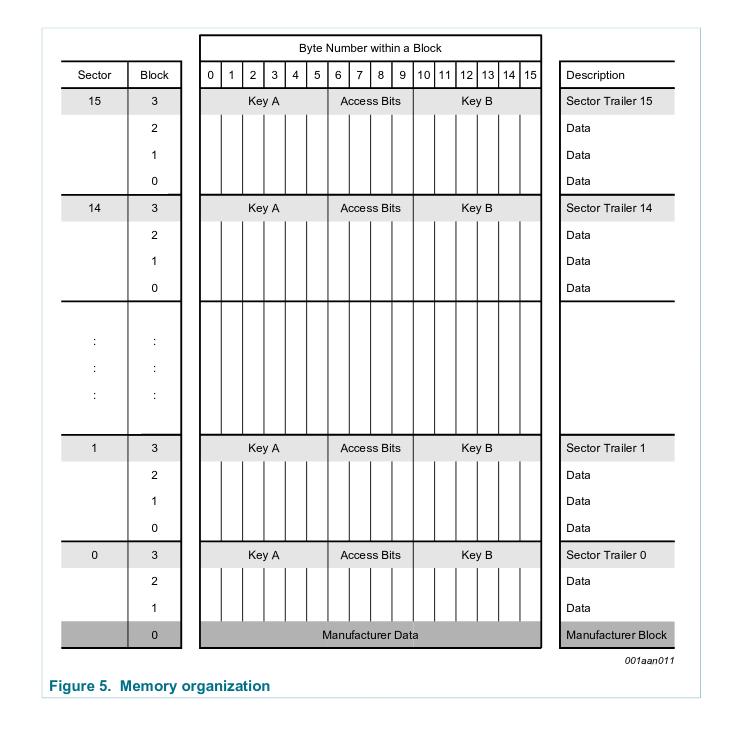
The 1024 bytes are divided into 16 sectors. Each sector has been divided into 4 blocks. Here is what you need to know.
Each sector’s fourth (last) block holds access keys and permissions for the block. This block is called sector trailer block. You can’t use it like a data block except for the 10th byte in that block. I’ll explain the trailer block a bit later.
In order to access the data in a sector you need to authenticate yourself with either key A or key B. The sectors trailer can tell you which key you should use for which operation (read/write).
The first block of the first sector holds manufacturer data, including the UID, but if you can read contents of this sector, that means you already know PICC’s UID.
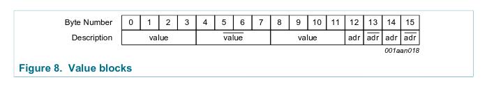
The data blocks can be treated as a simple memory storage. You write into those and you read from them. All 16 bytes of a data block are available. Those blocks can also be configured to function as value blocks. This type of a block uses 16 bytes to store 4 byte value. Sounds inefficient but the idea here is to store a value in a reliable way. The reliability comes from using: 8 bytes to hold a copy and a bit inverted copy of that value, 4 bytes to hold storage address for the block (the address uses only 1 byte but it’s copies take 3 more bytes).
Value blocks take an entire block to store one, 32 bit value. Those blocks have additional operations over read and write. User can increment/decrement, transfer/restore the stored value. Incrementing or decrementing the value puts the new value in the Internal Transfer Buffer. Next step would be to use a transfer operation to write the contents of the Internal Transfer Buffer back into value block. Restore operation reads the value stored in a block into Internal Transfer Buffer.
How to configure the data block to be a value block? Just use the data format shown below. There is no explicit configuration outside of adhering to this data format.
Ok, you want to write to or read from the memory block. Before you can do that you need to authenticate. You need to authenticate per sector - makes sense since the permissions are specified in the sector trailer. That means you can write into multiple blocks, in the same sector, after successful authentication, but you can’t operate on multiple sectors without going through the authentication procedure for each of the sectors you want to access.
The authentication procedure is pretty complicated. It’s called a Three Pass Authentication Sequence and if something uses three steps, you know it’s real engineering. Fortunately the RFID readers make this step pretty simple. I’ll discuss the actual steps one has to take when discussing specific RFID readers. At this point it’s important to reiterate that authentication can be done with one of two keys: key A or key B.
The part of the security that’s important to understand is encoded in the sector trailer.
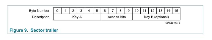
First six bytes hold the A key and the last 6 bytes hold the B key. The 4 bytes in the middle (it’s actually only 3 - one byte can hold user data) describe which operations are allowed on a specific block for a specific key used during authentication - called Access Bits.
Sector trailer is readable… assuming you authenticated with the proper key. That means you have
to know the key before accessing the key… Fortunately the PICCs are produced with a default
keys baked in. For me, authenticating with FF FF FF FF FF FF worked well. Your default key might
differ but you should find common, default keys online.
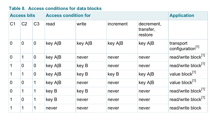
After successful authentication you’ve read a full sector, meaning full 4 blocks. The last block is the sector trailer. How to make sense of those 3 bytes which encode the access permissions? Look at the table, loudly say “What?”, start crying.
This animation helps me find a pattern in this mess. Depending on which block you’re interested in, you can extract the bits that describe that block, using this diagram. There is only 3 bits per block, which encode access permissions.
Now, depending on what you want to access, sector trailer or data block, you have to consult two more tables.
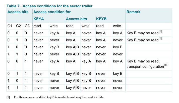
If you’ve authenticated with a key, which can’t access the keys in the sector trailer, attempting to read those keys, will return sector trailer bytes with key bytes zeroed out.
The actual authentication means transmitting an authentication command. The authentication command header is encoded with a different value when you authenticate with key A or key B. The rest of the command is the block address that the user wants to access and the last 4 bytes of the UID. Nothing here seems to be done in three steps - as the authentication sequence was supposed to be done. That’s because the complexity is abstracted away from the user. Building the correct authentication command as described above and passing it to the RFID reader, to transmit it to the PICC is enough from the developer’s perspective.
I’ve mentioned that we control PICC’s state using commands. There are the Anticollision commands, security related commands and finally the memory related commands. The full set of supported commands for MIFARE chips can be found in the datasheet MIFARE Classic EV1 1K on page 13. Till now I’ve focused on explaining the steps without going into implementation details. It’s best to get into those details when going through the RFID reader driver implementation. It might be beneficial to skim through the commands implementation in order to understand differences between MIFARE and other types of PICCs.
NTAG <
When I begun my RFID learning journey I’ve started with the MIFARE tags. It took a while to wrap my head around it and write a RFID reader driver which handles those type of PICCs. I wanted to order very small PICCs for my project and I was able to order several, round (8mm in diameter) MIFARE chips. They were too small for my reader to pick them up reliably so I went back to searching for slightly bigger ones. I’ve realized that it’s very difficult to find small MIFARE PICCs. Plenty of the NTAG family chips were available. I wasn’t too happy about it since that meant I needed to add NTAGs handling code.
Little did I know! NTAGs are way simpler than MIFAREs. A lot of functionality is shared so the code didn’t need that much work. If you need PICCs for your project, I can assure you that NTAGs are an improvement over MIFAREs, for most needs.
The NTAG family fully complies with the ISO 14443A and NFC Forum Tag Type 2 and 4 specifications. That means that the process of selecting (Anticollision) the PICC is exactly the same for the MIFARE and NTAG PICCs. The thing that you need to know is that all the NTAG chips (NTAG213, NTAG215, NTAG216) have a 7 byte long UID. Meaning that you have to send the Select command twice to see the PICC respond with SAK and go into the active state.
The diagram above, taken from the NTAG datasheet, shows the internal states of the chip. This is a stark improvement over the MIFARE’s diagram. This diagram actually shows the steps I’m describing pretty clearly.
The entire security functionality of those PICCs is turned off by default. The authentication procedure is different for MIFARE and NTAG. Lets first explore the default setup in which you don’t have to worry about the security.
Since the security is turned off, you can access the memory contents immediately after selecting the PICC. The selecting procedure is the same as for MIFARE but you just skip the authentication part. The memory itself is laid out in a very different way than the memory of the MIFARE chips.
NTAG memory <
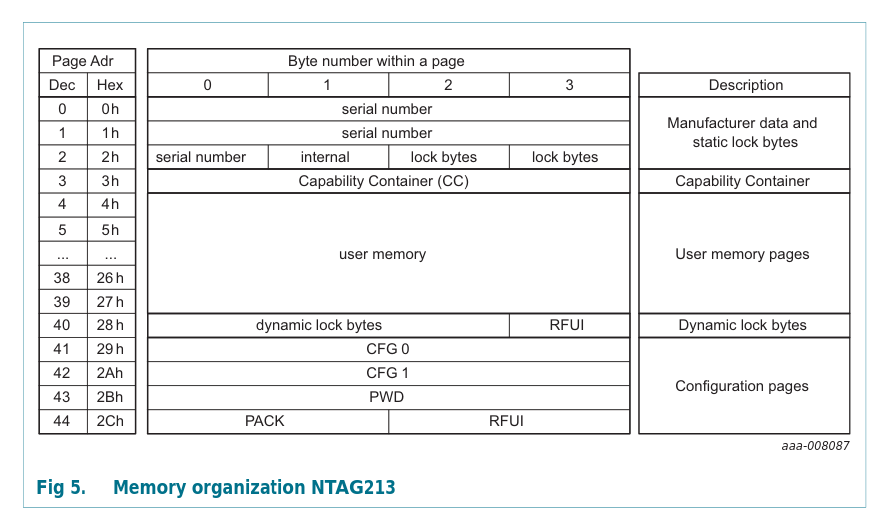
The memory unit of the NTAG chips is a page, which holds 4 bytes of data. The NTAG213 holds 144 bytes of user data (36 pages), the NTAG215 496 bytes and NTAG216 872 bytes. Huh, what to do with all those bytes???
Since the user memory is continuous and the secure access is simplified, the read/write operations are simpler. When reading, you can read the entire memory after one Select command. You don’t have to HALT the PICC between each read and you don’t have to skip (or ignore) the sector trailer since there is none. You can just read the entire memory space in a single loop! Technology came so far! The only changes I had to introduce in my code to be able to read NTAG memory was to skip the authentication step and to correctly address the memory pages.
There is an important reason for why it worked - the pool of supported commands. If you look at the
NTAG datasheet page 32 you’ll see all the available commands NTAG supports.
There you’ll see the READ command. You can compare it with the MIFARE Classic EV1 1K
page 13. In both cases the READ command is encoded with the value 0x30. For both types of
PICCs this command reads 16 bytes of data. What you might notice is the FAST_READ command
which only shows up in the NTAG datasheet. Since the memory structure of NTAG is continuous
it was easier to implement a read command which allows for reading a longer chunk of data
than only 16 bytes.
While we’re at it, it’s worth pointing out the GET VERSION command. Again, you’ll find that one only in the NTAG datasheet. For MIFARE you can establish the type of the PICC by analyzing the contents of the SAK response. NTAG has a dedicated GET VERSION command for that. Your software should know the type of the PICC it handles and its memory layout and size. Thus, important stuff!
Writing into NTAG can also be done with the WRITE command that MIFARE uses. When writing into MIFARE you have to write a 16 byte buffer. On NTAG the memory is partitioned into 4 byte pages. Thus, using this WRITE command on the NTAG will result in writing only 4 least significant bytes of the 16 bytes buffer. The WRITE command I’m describing here is called COMPATIBILITY WRITE in the NTAG datasheet.
The COMPATIBILITY WRITE command is split into two stages: sending the memory block address, sending the actual data. Using this type of writing on the NTAG didn’t work well for me. The data written into the memory was malformed. It might have been a timing issue. The first stage takes 5ms while the second stage takes 10ms. It works well on MIFARE so instead of debugging it on the NTAG PICCs I’ve implemented the native WRITE command of the NTAG chip. This command sends the memory page address and the data in the same packet. COMPATIBILITY WRITE expects 16 bytes buffer but writes only 4 bytes. The native NTAG WRITE command expects 4 bytes buffer. This command takes 10ms. That saves 5ms per write compared to the COMPATIBILITY WRITE. After using this command the stored data looked correct.
NTAG doesn’t have the concept of value blocks. It has an additional feature of a 24 bit counter which increments on each READ or FAST_READ command. Several more, less interesting features, are available which I won’t mention here.
Let me quickly explain the security features. If you look at the contents of the last 4 pages you’ll
find a CFG 0 page. The third byte of this page holds the AUTH0 byte. This byte holds the
address of the first, password protected memory page. By default it’s set to 0xFF which basically
disables the password protection. If you set this value to 0x05 then each page with address equal
or higher than 0x05 will require password authentication before reading or writing their contents.
Before you set the AUTH0 value, you should write a 4 byte password into the PWD page and the 2 byte password acknowledgement into the PACK page. You can never read values of the PWD and PACK. You can write freely into those, unless the AUTH0 byte holds and address equal or lower than the PWD page. It is possible to configure the security to protect from read/write or only write operations.
If the security has been configured, accessing protected memory needs to be preceded with an authentication command PWD AUTH. You better remember what you’ve written in the PWD page.
You can find more about memory locking without authentication in the NTAG datasheet. I haven’t touched on all of the NTAG features but this is the most important part. The optional security and a reasonable memory layout make these chips way easier to work with.
Readers - THIS PART OF THIS POST IS STILL WORK IN PROGRESS <
Lets talk about the readers! The most popular reader is based on the MFRC522 chip. Readers based on this chip are cheap and you can find them everywhere. Fun fact? They are broken. The readers’ modules, not the chips themselves. What do I mean by broken? Give this a read.
If the link is down:
MFRC522 datasheet says that max TX current is 150mA, but measured current was only 7mA. I have a very good RF design experience so I started to measure whole RF part and make full tuning. And what I found, antenna is tuned, not perfectly but usable, so was matching circuit. But used 2.2uH inductors does not meet with required parameters. Solution: Replace inductors L1 and L2 with same inductance (2.2uH) but higher operating current (like 200mA). … C4 and C5 must be changed. Replace them with 33pf capacitors.
I did try those modifications and it certainly improves this reader’s reliability and range. We usually take it for granted that if we buy a module like it should work properly, right? Well we’re all just people doing people things, mistakes included. If you want to use this reader consider resoldering those components. It does make a difference. The guy who posted this solution? I salute you!
MFRC522 <
Some dry facts about this chip:
- supports ISO/IEC 14443 A/MIFARE and NTAG - certainly good to know.
- supports SPI, I2C and UART communication - gives the user some flexibility.
- CRC coprocessor - a neat feature which is used in a lot of open source libraries.
- FIFO buffer handles 64 byte send and receive - worth knowing when writing a driver.
- made by NXP - good for you NXP!
The MFRC522 documentation will dazzle you with other fancy features.
Lets go through the actual communication with the MFRC522. I have only used SPI bus so the explanation is based on the experience with that interface. I was able to reliably communicate with the MFRC522 with half duplex SPI working at 10MHz.
The MFRC522 has a series of configuration registers. In order to write or read from the registers the data for the SPI transfer needs to: have the bit 0 set to 0, bits 1-6 set to the register address that’s about to be read from or written to, bit 7 set to 1 for read operation or to 0 for write operation.
For example, the data buffer for writing into ModWidthReg (the register naming taken from the
datasheet) would look like so:
{
  // ModWidthReg address is 0x24.
  const uint8_t reg_addr = 0x24;
  uint8_t data[2];
  // Bit 0 set to 0, bit 7 set to 0 (write operation).
  data[0] = (reg_addr << 1) & 0b01111110;
  // Write 0x25 in the register.
  data[1] = 0x25;

  spi_transfer(data);
}
I’ll only explain the registers that I’m using when interfacing with the MFRC522.
How would you go about actually transmitting the data between the reader and the PICC? First you need prepare the MFRC522, then you load its FIFO buffer and set the command to the transmit command. Then you toggle the bit! The bit that releases all that data into the world.
void rc522_transmit(uint8_t* const data,
                    const uint8_t data_size,
                    response_t* const response)
{
  const uint8_t cmd = RC522_CMD_TRANSCEIVE;

  const uint8_t irq = 0x77; // 0b1110111
  const uint8_t irq_wait = 0x30; // RxIRq | IdleIRq

  // Enable passing the interrupt requests. 0x80 turns on the HiAlert which
  // triggers when the FIFO is almost full (WaterLevel is the limit).
  // The WaterLevel isn't set anywhere here.
  rc522_write(RC522_REG_COM_IRQ_EN_DI, irq | 0x80);
  // Clear the HiAlert.
  rc522_clear_bitmask(RC522_REG_COM_IRQ, 0x80);
  // 0x80 = flush the FIFO buffer.
  rc522_set_bitmask(RC522_REG_FIFO_LEVEL, 0x80);
  // Change to IDLE mode to cancel any command.
  rc522_write(RC522_REG_COMMAND, RC522_CMD_IDLE);
  // Write the data into FIFO buffer.
  rc522_write_n(RC522_REG_FIFO_DATA, data_size, data);

  rc522_write(RC522_REG_COMMAND, cmd);

  // TRANSMIT THE DATA!!!
  rc522_set_bitmask(RC522_REG_BIT_FRAMING, 0x80);

  uint16_t dont_lock = 1000;

  while (1)
  {
    uint8_t interrupt_bits = rc522_read(RC522_REG_COM_IRQ);

    // Check for possible interrupts.
    if (interrupt_bits & irq_wait)
    {
      break;
    }

    // It might be a timeout.
    if (interrupt_bits & 0x01)
    {
      break;
    }

    if (--dont_lock == 0) break;
  }

  // Stop the transmission to PICC.
  rc522_clear_bitmask(RC522_REG_BIT_FRAMING, 0x80);

  if (dont_lock != 0)
  {
    // Check for 0b11011 error bits.
    if((rc522_read(RC522_REG_ERROR) & 0x1B) == 0x00)
    {
      // Check how many bytes are in the FIFO buffer. The last one might be an incomplete byte.
      response->size_bytes = rc522_read(RC522_REG_FIFO_LEVEL);
      // Returns the number of valid bits in the last received byte. The response might have been
      // smaller than 1 byte.
      const uint8_t last_bits = rc522_read(RC522_REG_CONTROL) & 0x07;
      if (last_bits == 0)
      {
        response->size_bits = response->size_bytes * 8U;
      }
      else
      {
        response->size_bits = (response->size_bytes * 8U) - (8 - last_bits);
      }

      if (response->size_bytes)
      {
        // Using the second half of the scratch_mem for incoming data.
        response->data = (scratch_mem + 2 * (SCRATCH_MEM_SIZE / 3));
        // Read the data into scratch memory.
        for(uint32_t j = 0; j < response->size_bytes; j++)
        {
          response->data[j] = rc522_read(RC522_REG_FIFO_DATA);
        }
      }
      else
      {
        response->data = NULL;
      }
    }
  }

  return;
}