[STM32] - part 2 - Lets look inside!
Still wondering why it all works? Why this black square does things? Lets go deeper.
Previously I explained a bit about processor architecture. It’s the basis of the chip. It’s a fundament. You won’t find anything about an UART in a Technical Reference Manual of Cortex-M4. It’s just not a part of this fundament.
When you get an STM32 microcontroller based on the Cortex-M4 architecture you just get microcontroller made by ST which uses this specific architecture. What stops them to add to it? Nothing. That’s why you can find so many different models of families and models of processors. Just look at ST’s F and ST’s L series. They are both ARM Cortex-M but they do differ in many ways.
Lets look at what are those from the perspective of someone who programs microcontrollers.
It’s all in the memory <
As long as you just need to crunch some numbers the basic structure of the microcontroller is enough - that’s the ARM architecture implementation with the arithmetic logic unit. Without external interface you don’t have any input or output. Without any input periphery even programming the controller is impossible, because how would you transfer your instructions into its memory?
In order to learn more lets open STM32F303x6/x8 microcontroller datasheet.
On page 13 you can read a short description:
The Arm 32-bit Cortex -M4 RISC processor with FPU features exceptional co de-efficiency, delivering the high performance expected from an Arm core, with memory sizes usually associated with 8- and 16-bit devices. The processor supports a set of DSP instructions that allows efficient signal processing and complex algorithm execution.
Its single precision FPU speeds up software development by using metalanguage development tools, while avoiding saturation.
Neat.
At the same page you can find summary of the memories types and its sizes. To see exactly how the memory is organized head to page 42. I have attached the image of this page below.
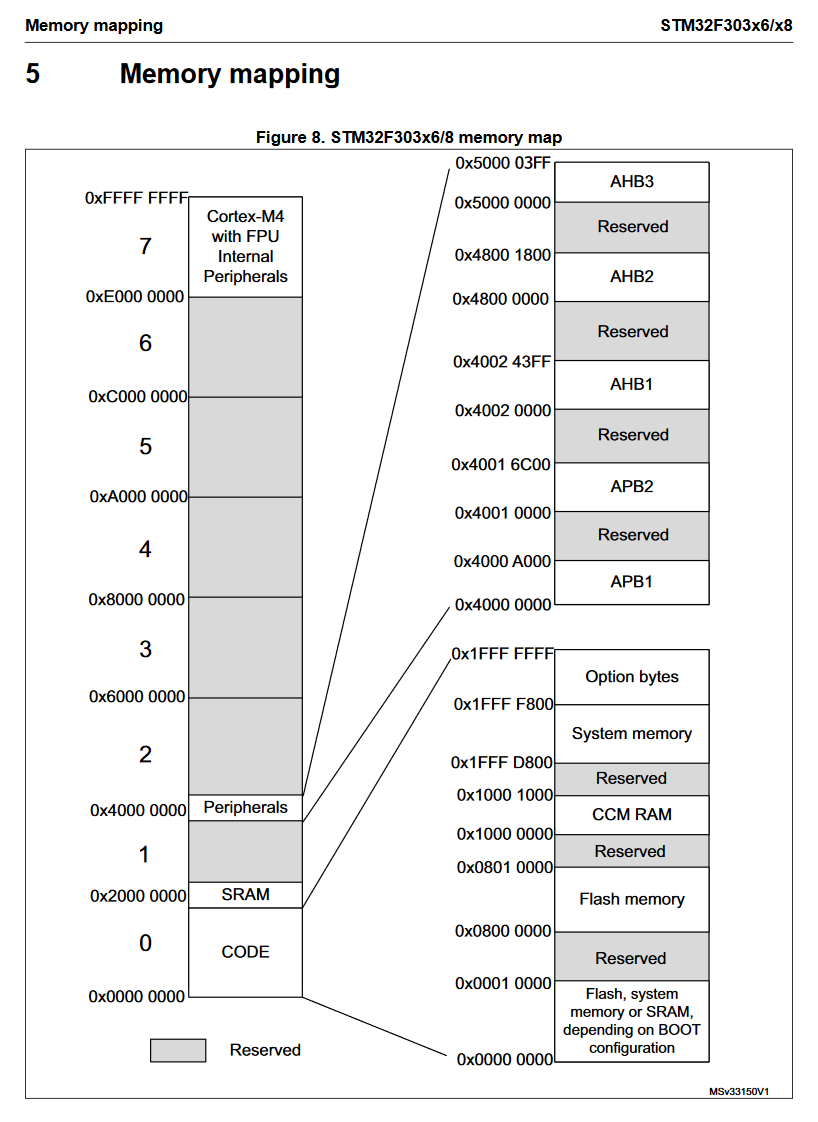
This schematic shows the full memory layout. Grey cells represent reserved memory - meaning, not to be used. Starting from the address 0x0000 0000 you can see the part of the memory called CODE. It’s broken down into smaller chunks. Among those chunks you will find a chunk called Flash memory. It starts at 0x0800 0000 and ends at 0x0801 0000. That would give a flash memory of 0x0001 0000 (65536 in decimal) which equals to 64KB (K = 1024).
The next section is SRAM memory. According to the datasheet this one is 12KB. I will get into more detail in the future but this part of the memory is used to store data runtime. When the processor is powered off, code and data resides in flash memory, but when you start the processor it goes through a reset interrupt handler - small code written in Assembler which sets everything up by copying data from FLASH to SRAM (it also does other stuff like setting up the stack pointer address but we will get into it later).
Notice that SRAM memory holds only 12KB. That’s not a lot compared to the FLASH memory which can hold 64KB. By default, the microcontroller fetches the instructions directly from the FLASH memory, via the ICode bus. It doesn’t need to copy it into SRAM. Only data gets copied. That saves the precious SRAM memory. This is called Execute In Place or XIP in short. It’s possible to execute instructions from the SRAM memory but it’s rarely used.
The last part of the memory I want to discuss is the Peripherals. It splits into 5 smaller chunks with Reserved memory in between them. Those chunks are: APB1, APB2, AHB1, AHB2, AHB3. Those parts of the memory are described just below the memory map. You will find for example that GPIOA, responsible for the pins connected to the A port, are controlled by registers accessible via the AHB2 bus (a bunch of memory mapped registers). What do I mean by controlled? Imagine this AHB2 memory space is just a row of switches, where every switch represents a bit. By flipping those bits to either 1 or 0 you can control specific parameters of the peripherals. You need to change baud rate of a serial communication on USART1 port? From table 16 you know the configuration bits are in 0x4001 3800 - 0x4001 3BFF space.
There isn’t much more in the memory… Just a bunch of reserved space (what’s there I wonder… anything? nothing?1). There is also this ARM fundament I was writing about - ARM Cortex-M4 with FPU Internal Peripherals… because as I have said:
Everything comes down to memory. Processors just read and write from and to memory. <
Links worth checking out:
- Programming manual - this one goes really deep. A lot of Assembler examples.
- Here you can find everything a developer needs about STM32F303xB/C/D/E, STM32F303x6/x8, STM32F328x8, STM32F358xC and STM32F398xE microcontroller memory and peripherals. 1141 pages…
STM32 Explained part 1 STM32 Explained part 3
-
I have received an answer to this question. I will cite it because I think it’s really interesting and worth repeating: To answer that question a bit: probably some “private” bits for the peripherals to work with and on the “smaller” devices these can be spots where optional peripherals would be, and sometimes they are actually there. The ST-link-V2 clones feature a STM32F100 device which officially does not support USB, however, they just seem to work fine connecting to a USB port. The USB controller probably did not pass some tests and therefore they labeled the chip as one without a USB controller. Same as with some graphics cards that can be flashed with a BIOS of a higher version. The larger blocks are just not used I guess. - Thomas Gravekamp, check his stuff here. ↩︎